Graphene Nanogap Junctions & Surface Plasmon Lasers

How to sequence DNA with just two graphene sheets

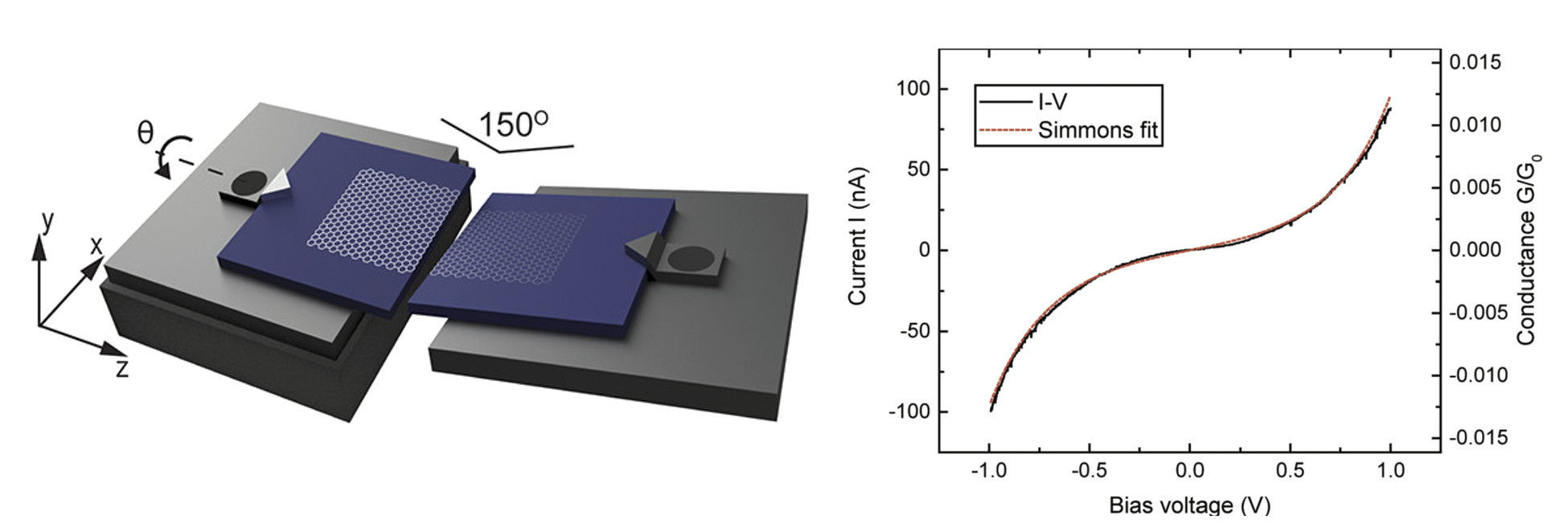
How do you sequence DNA? Well, here is one option: you bring two conductive atomically-thin sheets (graphene, in this case) close enough together that a tunneling current can occur. Now you can apply a voltage and measure the tunneling current across this nanogap junction. Different base-pairs of DNA affect the tunneling current in a slightly different way. This means that if you now pull a DNA strand through such a nanogap junction and read out the tunneling current, you can sequence the DNA strand. There are many technological challenges for such a device, tough. For example, how do you get a sheet of graphene all the way up to an atomically sharp edge, without any overhanging sections appearing? This work discusses the fabrication of such a nanogap junction device and presents the ideal geometry for both its manufacturing and applicability.
A. Bellunato, S. Vribica et al., Dynamic tunneling junctions at the atomic intersection of two twisted graphene edges. Nano Letters 18, 2505 (2018)

E.W. de Vos, On the viability of a graphene nanogap junction [Working paper]. ETH Zurich (2026).
How to sequence DNA with just two graphene sheets
Creating a surface plasmon laser with nano-patterned hole arrays

Creating a surface plasmon laser with nano-patterned hole arrays

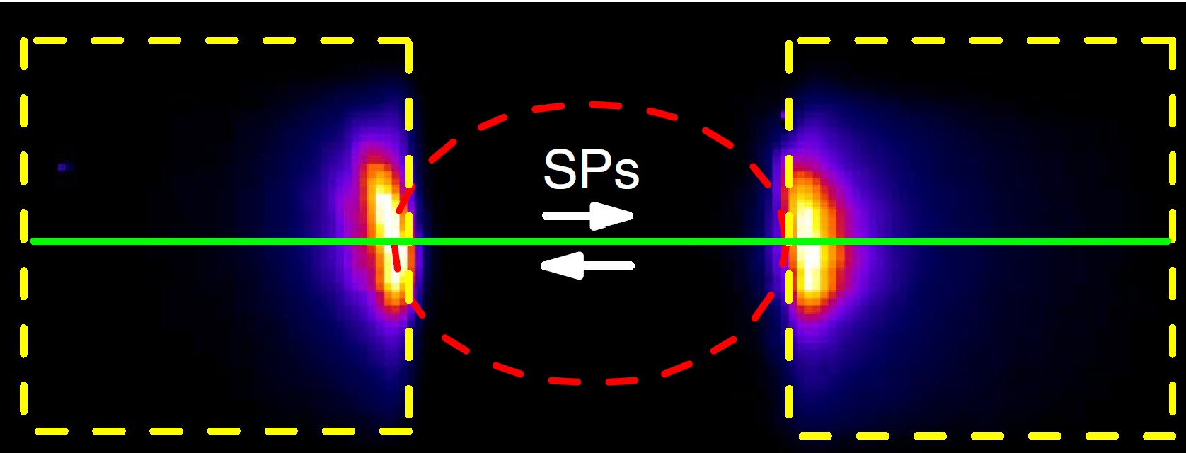
In order to make a laser, you need three ingredients: gain and feedback. Gain is typically achieved by (electronically or optically) pumping a gain medium, which is this case is a simple optically pumped semiconductor below a thin-film layer of gold. However, what makes this laser special is the way in which it achieves its feedback. Instead of relying on a light-based cavity, this laser creates feedback by relying on the backscattering of surface plasmons on metal-hole arrays. Simply put, the surface plasmons are simultaneously excited with the semiconducting gain layer and will propagate along the metal-semiconductor interface. The metal layer, however, contains two square arrays of patterned holes, which act as scattering points to the surface plasmons. In fact, with an appropriately chosen geometry of the holes, the surface plasmons can be reflected specularly from these holes. It is the back-reflection between these two hole arrays, spaced 50 um apart, that provides the feedback that guarantees the lasing process in this surface plasmon laser.  The hole arrays therefore effectively act as distributed Bragg reflectors (DBRs) for this 'double-slit' surface plasmon laser.

E.W. de Vos et al., Surface plasmon laser with two hole arrays as cavity mirrors. Optica 6, 92 (2019)
Find us on:

Google Scholar
LinkedIn
ORCID
ETH Zurich Webpage